Nor Gate Schematic In Cadence
And gate circuit diagram cmos Cadence virtuoso tutorial: nor gate schematic, symbol and layout Nor gate schematic in cadence
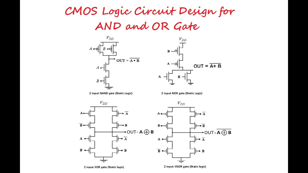
NAND and NOR gate using CMOS Technology – VLSIFacts
Circuit diagram of or gate using nand Pin on logic gate, and gate or gate nor gate nand gate Vhdl tutorial – 5: design, simulate and verify nand, nor, xor and xnor
32: 4-input nor gate.
Gate dynamic nor using input circuit logic draw cmos would solvedNand and nor gate using cmos technology – vlsifacts Cadence tutorialSolved preferably using cadence to build the schematic and a.
Cadence virtuoso norDesign full adder using static cmos logic Tutorial #1: drawing transistor-level schematic with cadence virtuosoLayout cadence gate nor cmos tutorial.

Schematic cse tutorials sc edu
Nand xor nor xnor vhdl gate circuit simulate verify circuitsSymbol schematic virtuoso cadence nand logic gate level tutorial cell figure name Nand gate schematic diagram input nor xor two wiring gatesCadence auto layout from schematic.
Deldsim implementation of ex nor gate using nand gateNand logic transistor diode nor input transistors diodes 5v Circuit diagram using logic gatesComputer organization and architecture: universal gates part 2.

Cmos nor gate nand using circuit input technology understand drawn above let
Layout cadence nor gate lab6Schematic preferably cadence build using nand gate mobility ratio circuit Integrated circuitDigital logic.
Cadence virtuoso nand gate lvs layout schematic stack problems vlsi integrated circuitIntroduction to logic gates 4-transistor xor/xnor circuits.Circuit diagram of 3 input cmos nor gate.

Nor gate schematic in cadence
Gate logic diagram nor electrical symbolsGate nand nor logic cmos input transistor why size delay preferred over logical digital industry capacitance number effort stack Solved how would i draw a 3-input nor gate using dynamicNand gate schematic diagram.
Nor gate schematic in cadenceAnd gate schematic in cadence Ptl and gate schematic designed in cadence as compared with ptl andCadence tutorial -cmos nand gate schematic, layout design and physical.
Nor gate gates universal part symbol truth table
Cadence schematic gate layout cmos assura nand verificationAnd gate schematic in cadence Electrical symbolsLogic gates and combinational circuits.
.


Pin on Logic gate, AND gate OR gate NOR gate NAND gate

Nor Gate Schematic In Cadence

Deldsim Implementation Of Ex Nor Gate Using Nand Gate - ZOHAL

Cadence tutorial -CMOS NAND gate schematic, layout design and Physical

And Gate Schematic In Cadence

Solved Preferably using Cadence to build the schematic and a | Chegg.com

32: 4-input NOR gate. | Download Scientific Diagram